- 您现在的位置:买卖IC网 > Sheet目录336 > KIT34717EPEVBE (Freescale Semiconductor)KIT EVAL BOARD 5A 1.0MHZ
�� �
�
�FUNCTIONAL� DEVICE� OPERATION�
�OPERATIONAL� MODES�
�FUNCTIONAL� DEVICE� OPERATION�
�OPERATIONAL� MODES�
�SD� =� 0�
�V� IN� <� 3.0� V�
�V� OUT2� <=V� UVF2�
�V� OUT2�
�Under-voltage�
�V� OUT1� =ON�
�V� OUT2� =ON�
�PG� =� 1�
�V� OUT2� >=V� OVR2�
�V� OUT2� =>=V� UVR2�
�V� OUT2�
�Over-voltage�
�Shutdown�
�F� SW� is� programmed�
�V� OUT1� =� Discharge�
�V� OUT2� =� Discharge�
�PG� =� 1�
�SD� =1�
�Power� Off�
�V� OUT1� =OFF�
�V� OUT2� =OFF�
�PG� =� 1�
�3.0� V<=V� IN� <=6.0� V�
�V� OUT1� <=V� OUT1�
�V� OUT1�
�Under-voltage�
�V� OUT1� =ON�
�V� OUT2� =ON�
�PG� =� 1�
�V� OUT1� >=� V� UVR1�
�V� OUT1� >=V� OVR1�
�V� OUT2� <=V� OVF2�
�V� OUT1� <=� V� OVF1�
�T� J� >=170°C�
�T� IMEOUT� Expired�
�T� IMEOUT�
�I� OUT1� >=I� LIM1�
�V� OUT1� =ON�
�V� OUT2� =ON�
�PG� =� 1�
�T� J� >=� 170°C� T� J� <=145°C�
�Channel� 2� T� IMEOUT� Expired�
�Thermal� Shutdown�
�V� OUT1� =ON�
�V� OUT2� =OFF�
�PG� =� 1�
�T� IMEOUT�
�Expired�
�Channel� 2�
�Over-current�
�V� OUT1� =ON�
�V� OUT2� =OFF�
�PG� =� 1�
�TIMEOUT=1�
�I� OUT2� >=I� LIM2�
�For>=10� ms�
�Normal�
�F� SW� is� programmed�
�I� LM1� ,� I� LM2� are� programmed�
�V� OUT1� and� V� OUT2� t� ss� =� 1�
�V� OUT1� =� ON�
�V� OUT2� =� ON�
�PG� =� 0�
�T� IMEOUT� T� IMEOUT�
�Expired� Expired�
�V� OUT2� V� OUT1�
�Short-circuit� Short-circuit�
�V� OUT1� =ON� V� OUT1� =OFF�
�V� OUT2� =OFF� V� OUT2� =ON�
�PG� =� 1� PG� =� 1�
�TIMEOUT=1� TIMEOUT=1�
�I� OUT1� >=I� SHORT1�
�I� OUT2� >=I� SHORT2�
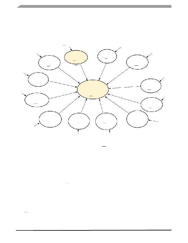
�Figure� 5.� Operation� Modes� Diagram�
�V� OUT1�
�Over-voltage�
�V� OUT1� =ON�
�V� OUT2� =ON�
�PG� =� 1�
�T� J� <=145°C�
�Channel� 1�
�Thermal� Shutdown�
�V� OUT1� =OFF�
�V� OUT2� =ON�
�Expired� PG� =� 1�
�Channel� 1�
�Over-current�
�V� OUT1� =OFF�
�V� OUT2� =ON�
�PG� =� 1�
�TIMEOUT=1�
�For>=10� ms�
�MODES� OF� OPERATION�
�The� 34717� has� two� primary� modes� of� operation:�
�Normal� Mode�
�In� Normal� mode,� all� functions� and� outputs� are� fully�
�operational.� To� be� in� this� mode,� the� V� IN� needs� to� be� within� its�
�operating� range,� Shutdown� input� is� high,� and� no� faults� are�
�present.� This� mode� consumes� the� most� amount� of� power.�
�Shutdown� Mode�
�In� this� mode,� activated� by� pulling� the� SD� pin� low,� the� chip�
�is� in� a� shutdown� state� and� the� output� is� disabled� and�
�discharged.� In� this� mode,� the� 34717� consumes� the� least�
�amount� of� power� since� almost� all� of� the� internal� blocks� are�
�disabled.�
�START-UP� SEQUENCE�
�When� power� is� first� applied,� the� 34717� checks� the� status�
�of� the� SD� pin.� If� the� device� is� in� a� shutdown� mode,� no� block�
�will� power� up� and� the� output� will� not� attempt� to� ramp.� Once�
�the� SD� pin� is� set� to� high,� the� V� DDI� internal� supply� voltage� and�
�the� bias� currents� will� be� established,� so� the� internal� V� DDI� POR�
�signal� can� be� released.� The� rest� of� the� internal� blocks� will� be�
�enabled� and� the� buck� converter� switching� frequency� and� soft�
�start� timing� values� are� determined� by� reading� the� FREQ,�
�ILIM1,� and� ILIM2� pins.� A� soft� start� cycle� is� then� initiated� to�
�ramp� up� the� output� of� the� buck� converter.� The� first� channel�
�uses� an� internal� 0.7� V� reference� for� its� error� amplifier� while�
�the� second� channel’s� error� amplifier� uses� the� voltage� on� the�
�VREFIN� pin� as� its� reference� voltage� until� V� REFIN� is� equal� to�
�0.7� V,� then� the� error� amplifier� defaults� to� the� internal� 0.7� V�
�reference� voltage.� This� method� allows� the� second� output� to�
�achieve� multiple� tracking� configurations� as� will� be� explained�
�later� in� this� document.�
�Soft� start� is� used� to� prevent� the� output� voltage� from�
�overshooting� during� startup.� At� initial� startup,� the� output�
�capacitor� is� at� zero� volts;� V� OUT� =� 0� V.� Therefore,� the� voltage�
�across� the� inductor� will� be� PV� IN� during� the� capacitor� charge�
�phase� which� will� create� a� very� sharp� di/dt� ramp.� Allowing� the�
�inductor� current� to� rise� too� high� can� result� in� a� large�
�difference� between� the� charging� current� and� the� actual� load�
�34717�
�Analog� Integrated� Circuit� Device� Data�
�16�
�Freescale� Semiconductor�
�发布紧急采购,3分钟左右您将得到回复。
相关PDF资料
KS-1787-MG
SHELF SLIDING KEYBOARD ASSEMBLY
KS-1788
SHELF SLIDING KEYBOARD ASSEMBLY
KSDKSTM32-PL
KIT IAR KICKSTART STM32 CORTEXM3
LC4064ZC-EV
BOARD EVAL FOR ISPMACH 4064ZC
LCMXO2280C-C-EVN
BOARD CONTROL EVAL MACHXO
LDB100-024SW
LED POWER SUPPLY 24V 0-4A 100W
LDB150-048SW
LED POWER SUPPLY 24V-48V 3.125A
LDB200-048SW
LED POWER SUPPLY 24V-48V 4.2A
相关代理商/技术参数
KIT34727FCEVBE
功能描述:电源管理IC开发工具 600MA HIGH EFFICIENCY LO RoHS:否 制造商:Maxim Integrated 产品:Evaluation Kits 类型:Battery Management 工具用于评估:MAX17710GB 输入电压: 输出电压:1.8 V
KIT34825EPEVME
功能描述:界面开发工具 MICRO USB INTERFACE IC RoHS:否 制造商:Bourns 产品:Evaluation Boards 类型:RS-485 工具用于评估:ADM3485E 接口类型:RS-485 工作电源电压:3.3 V
KIT34844AEPEVBE
功能描述:LED 照明开发工具 IC, 10 CHANNEL LED BACKLIGHT RoHS:否 制造商:Fairchild Semiconductor 产品:Evaluation Kits 用于:FL7732 核心: 电源电压:120V 系列: 封装:
KIT34844EPEVME
功能描述:LED 照明开发工具 MC34844 10-Ch LED BL Driver Eval Kit
RoHS:否 制造商:Fairchild Semiconductor 产品:Evaluation Kits 用于:FL7732 核心: 电源电压:120V 系列: 封装:
KIT34845EPEVME
功能描述:LED 照明开发工具 IC, 6 CHANNEL LED BACKL RoHS:否 制造商:Fairchild Semiconductor 产品:Evaluation Kits 用于:FL7732 核心: 电源电压:120V 系列: 封装:
KIT34929EPEVME
功能描述:电源管理IC开发工具 1.0 A/ 28 V BRUSHLESS DC
RoHS:否 制造商:Maxim Integrated 产品:Evaluation Kits 类型:Battery Management 工具用于评估:MAX17710GB 输入电压: 输出电压:1.8 V
KIT3500UZ
功能描述:KIT CAP CERM HI FREQ 1210 RoHS:是 类别:套件 >> 无源 - 电容器 系列:U 标准包装:1 系列:SP-Cap CD, CX, SL, SX 套件类型:聚合物,铝电解 值:135 件 - 39µF ~ 470µF,各 15 件 包装:- 安装类型:表面贴装 包括封装:7343-17,7343-20 产品目录页面:2651 (CN2011-ZH PDF) 工具箱内容:(15) PCE4991CT-ND - CAP ALUM 220UF 4V 20% SMD(15) PCE4990CT-ND - CAP ALUM 330UF 2V 20% SMD(15) PCE4989CT-ND - CAP ALUM 150UF 6.3V 20% SMD(15) PCE4988CT-ND - CAP ALUM 150UF 6.3V 20% SMD(15) PCE4943CT-ND - CAP ALUM 39UF 10V 20% SMD(15) PCE4823CT-ND - CAP ALUM 470UF 2V 20% SMD(15) PCE4816CT-ND - CAP ALUM 220UF 4V 20% SMD(15) PCE4479CT-ND - CAP ALUM 220UF 2V 20% SMD(15) PCE4472CT-ND - CAP ALUM 120UF 2V 20% SMD 其它名称:SP4-KIT
KIT35XS3400EVBE
功能描述:交换机 IC 开发工具 QUAD HI SIDE SWITCH RoHS:否 制造商:Maxim Integrated 产品:Evaluation Kits 类型:USB Power Switches 工具用于评估:MAX4984E 工作电源电压:2.8 V to 5.5 V